Tesla and SpaceX aim for chip production in the millions
Tesla and SpaceX plan to reach a monthly manufacturing capacity of one million semiconductor wafers by 2032 with their joint factory, Terafab. A significant portion, namely 700,000 of these wafers, are intended for memory chips, roughly equivalent to Samsung’s current monthly DRAM production. The precise strategy to achieve this ambitious goal within just six years is currently unclear.
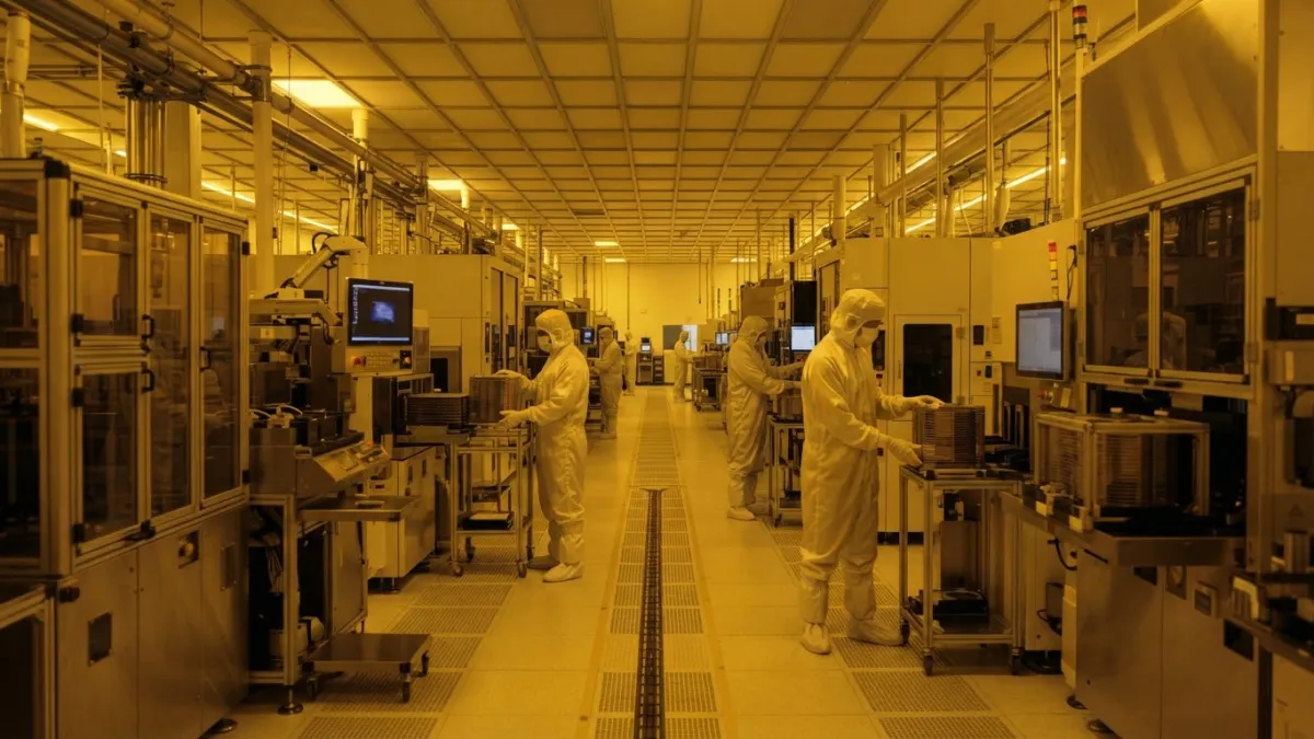
Terafab is intended to unite all phases of semiconductor production under one roof and is being realized with the support of Intel. The project aims to reduce dependence on external suppliers for AI chips and to build an independent infrastructure for processors and memory in the USA. The produced chips will be used, among other things, for Tesla’s humanoid Optimus robots and for the data centers planned by SpaceX in space.
According to the Japanese economic newspaper Nikkei, equipment manufacturers have already been informed about the expansion plans. According to the report, from 2032, 700,000 wafers per month will be intended for memory production and a further 300,000 for logic chips. Samsung’s current monthly DRAM capacity is approximately 650,000 to 700,000 wafers. It remains to be seen whether such an immense production capacity can actually be built up within the planned timeframe.
The first series production of functional chips is currently planned for the third quarter of 2028.
The investments to date in the semiconductor complex in Grimes County, Texas, amount to $16.8 billion. This figure appears relatively low considering the intended production volumes, which would correspond to the scale of a single new memory factory. Samsung has already invested hundreds of billions of dollars and will likely require further sums of a similar magnitude to double its capacity to 1.45 million wafers per month.
In the long term, Terafab is expected to cover an area of around 9.3 million square meters, which could make it the largest building in the world. In addition to manufacturing masks, lithography and chiplet packaging, the chips will also be tested directly in the factory in order to accelerate the development process and reduce the time from chip design to production from months to just a few weeks.
A possible cooperation with TSMC is once again under discussion after it had already been confirmed. Negotiations are now focused on operational control and investment conditions. Elon Musk previously described TSMC only as a foundry and rejected the company’s participation in Terafab.
Source
“Terafab: Elon Musk will 2032 monatlich 1 Million Wafer produzieren”
Read the original report (in German) ↗This story was written with AI tools from the original report credited above and published after automatic checks. No person read it before it was published. If you spot an error, please tell us: corrections are published on our corrections page. Read our editorial policy · Report an error · Corrections
Read next
Tesla and SpaceX stocks fall: future of planned merger uncertain
Shares of Tesla and SpaceX have fallen sharply, casting doubt on the future of a potential merger of the two companies owned by Elon Musk. Observers…
Related



Caught up in five lines
The Brief: the day’s biggest stories, written by our desk at and .